According to a source, Huawei has taken a big move and bravely moved forward under the US chip ban and started research in another field, namely photonic chips. The performance of this chip is better than existing chips and does not require lithography machines produced by European and American companies. The Dutch media commented on this that the US lithography machine blockade is meaningless, and China may not need this equipment to produce high-end chips in the future. At the same time, the Russian media also attached great importance to this move by Huawei. They said that the United States underestimated the strength and determination of Chinese companies, and the blockade would only arouse challenges from Chinese companies.
Blocking the lithography machine is meaningless
Recently, the White House has formulated a series of sanctions against Chinese semiconductor companies and communication technology companies. European and American companies are not allowed to sell goods or technologies to companies on the blacklist, including the Dutch ASML company. Manufacturing lithography machine. Huawei is one of the victims of these policies. The company’s business relies heavily on high-end chips produced in Europe and the United States, but the United States does not allow companies that own these chips to do business with Huawei.
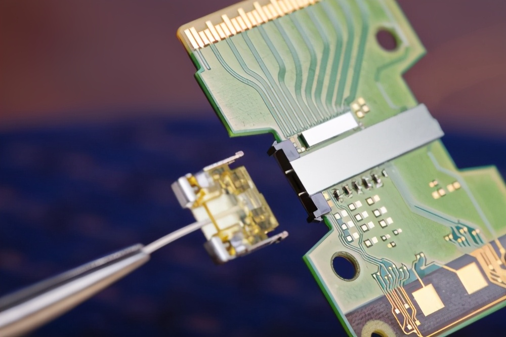
In order to break through this limitation, Huawei launched a big move and began to develop photonic chips. People who don’t know about chips may have never heard of such chips. In fact, there are many different sub-fields in the semiconductor industry. The familiar chips basically belong to the field of integrated circuits, while the photonic chip belongs to the field of optoelectronics. The latter is not well-known, but the performance of the chip is far better than ordinary integrated circuits.
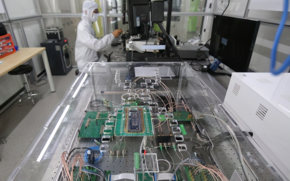
The advantage of the photonic chip is in the transmission performance, which can greatly improve the working efficiency of electronic equipment. Compared with traditional silicon chips, the advantages of photonic chips are very obvious. The data transmission of the entire photonic chip can reach an astonishing 300Gbps, which is 10-50 times that of current electronic chips. Not only that, the photonic chip may also break the shackles of Moore’s Law in the future. Although the current electronic chips have come to the 7nm/5nm process, it will be more and more difficult to rely on advanced technology to improve the performance and power consumption of the chips. When the limit is reached, traditional chip technology will face a bottleneck. Now the research on integrated circuits has gradually come to an end and is subject to physical boundaries. When the chip reaches the 2nm field, it is almost impossible to make a smaller chip. , Even if it succeeds, there is no guarantee that its performance will be greatly improved. On the whole, photonic chips are the future of the semiconductor industry.
If China takes the lead in breaking through the application of photonic chips, it can reverse its current disadvantages. In addition, this chip manufacturing process is completely different from the past. It does not require a lithography machine at all, and will use brand-new manufacturing technology. The Dutch media have discovered the most critical point. They claim that the US lithography machine blockade will soon lose its effect. In the future, we may not need these lithography machines at all.
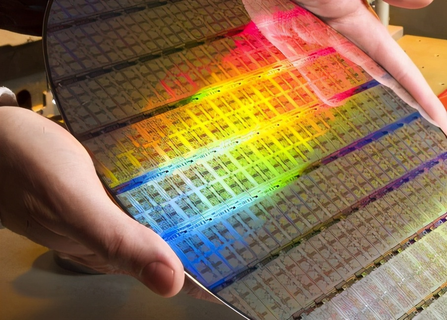
In addition to the layout of photonic chip research, Chinese companies have also prepared another magic weapon, namely carbon-based chips, more accurately graphene chips. Once this chip is successfully developed, it will completely overturn the development trajectory of previous chips. After more than ten years of intensive work in this field, the scientists of the Chinese Academy of Sciences have achieved beautiful results. The first batch of graphene wafers have been offline and the finished products have been displayed to the public, demonstrating China’s scientific research level.